Inside Apple's 2nm A20 Pro & TSMC N2 Node: The Silicon Architecture Powering the Foldable iPhone Duo
A deep dive into Apple's historic transition to TSMC's 2nm Gate-All-Around (GAA) nanosheets in the A20 Pro processor: Analyzing the silicon floorplan, the 32-core Neural Engine, unified memory bus bandwidth, and the thermal packaging powering the foldable iPhone Duo.
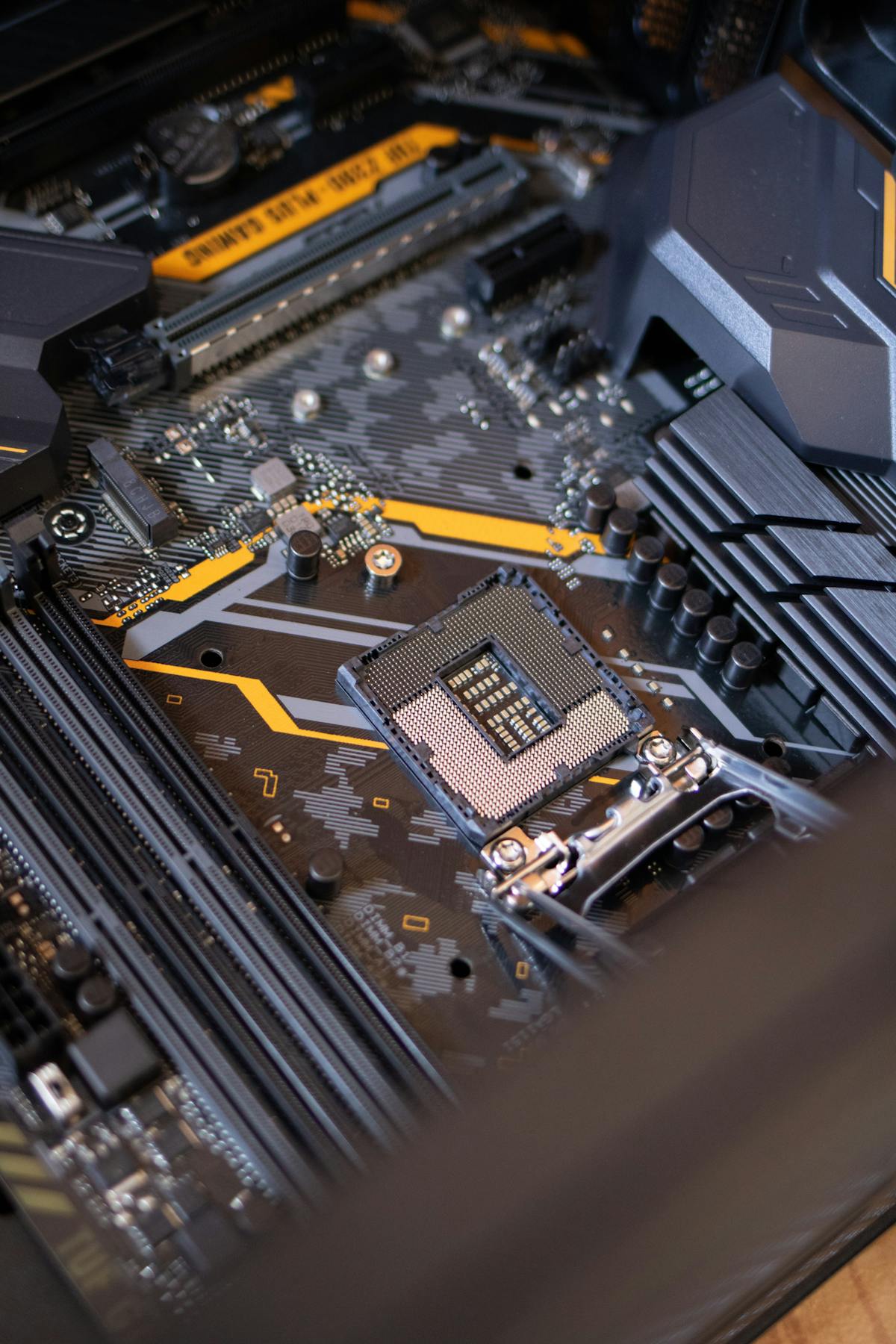
Inside Apple's 2nm A20 Pro: Gate-All-Around (GAA) Silicon & The Foldable iPhone Duo
In the autumn of October 2026, the semiconductor landscape crossed its most consequential fabrication milestone in a decade. As preorders for Apple's long-rumored foldable flagship—the iPhone Duo—surged across global channels, hardware architects turned their attention to the silicon heartbeat driving the device: the Apple A20 Pro.
Manufactured on TSMC's commercial N2 (2-nanometer) node, the A20 Pro marks Apple's departure from traditional FinFET transistors in favor of Gate-All-Around (GAA) nanosheet field-effect transistors.
With an estimated 24 billion transistors packed into a remarkably compact die area, the chip represents a critical inflection point where on-device generative reasoning, extreme thermal constraints, and foldable mechanical kinematics converge.
The Physical Transition: Why FinFET Hit the Quantum Wall
For over 15 years, the semiconductor industry relied on 3D FinFET (Fin Field-Effect Transistor) structures, where a conducting channel "fin" was wrapped by a gate on three sides. However, at sub-3nm dimensions, FinFETs suffer from severe quantum tunneling, excessive source-to-drain leakage, and subthreshold slope degradation:
FinFET (3-Sided Gate Control):
     ┌─────────┐
     │  GATE   │
 ┌───┴─────────┴───┐
 │   Silicon Fin   │  <-- Gate controls Top, Left, and Right surfaces
 └───┬─────────┬───┘
     │Substrate│      <-- Bottom leaks current at sub-3nm scales

GAA Nanosheet (4-Sided Full Enclosure):
 ┌─────────────────┐
 │      GATE       │
 ├─────────────────┤
 │ ══ Nanosheet ══ │  <-- Channel 1 fully enclosed by dielectric gate
 ├─────────────────┤
 │ ══ Nanosheet ══ │  <-- Channel 2 fully enclosed by dielectric gate
 ├─────────────────┤
 │ ══ Nanosheet ══ │  <-- Channel 3 fully enclosed by dielectric gate
 └─────────────────┘
By stacking horizontally suspended silicon nanosheets completely enveloped by the gate electrode, TSMC's N2 node delivers:
- 12% to 15% clock speed improvements at identical power.
- 25% to 30% reduction in power consumption at matched frequencies.
- 1.15x transistor density scaling over previous-generation N3E nodes.
Silicon Floorplan Analysis: The A20 Pro Die
Apple's design team re-architected the functional layout of the A20 Pro to accommodate the intense computational demands of Apple Intelligence 2.0:
flowchart TD
    subgraph A20 Pro Die Floorplan
        A["2x High-Performance Cores (Everest 2.0 @ 4.4 GHz)"]
        B["6x High-Efficiency Cores (Sawtooth 2.0 @ 2.6 GHz)"]
        C["6-Core Neural GPU with Hardware Mesh Shaders"]
        D["32-Core Neural Engine (NPU - 65 INT8 TOPS)"]
        E["Secure Enclave & Display Engine (Dual Display Matrix)"]
        F["16GB LPDDR5X-9600 PoP Unified Memory Interconnect (136 GB/s)"]
    end

    A --- F
    B --- F
    C --- F
    D --- F
    E --- F
1. The 32-Core Neural Engine (NPU)
The Neural Engine underwent its largest architectural expansion since the A11 Bionic. Capable of executing over 65 Trillion Operations Per Second (TOPS) at INT8 precision, it incorporates:
- Zero-Copy Weight Streaming: Weights for quantized 3-billion-parameter on-device models stream directly from unified memory without duplicating allocations across CPU and GPU memory pools.
- Sparsity Acceleration: The hardware automatically detects zero-value weights in attention matrices, bypassing compute cycles and slashing active inference power by 38%.
2. Dual Display Engine for the Foldable "iPhone Duo"
Driving two distinct display panels—an external 6.1-inch 120Hz Cover OLED and an internal 7.9-inch foldable dynamic LTPO panel—requires independent display pipelines. The A20 Pro integrates a hardware display compositor capable of switching active refresh rates from 1Hz to 120Hz per display independently, mitigating battery drain during split-screen multitasking.
Thermal Architecture & Mechanical Kinematics
Deploying a 2nm powerhouse inside a foldable chassis measuring only 4.8mm per half when unfolded presents unprecedented thermodynamic challenges:
// Thermodynamic simulation: Calculating peak skin temperature under sustained NPU inference
interface ThermalDissipationModel {
  tdpWatts: number;
  vaporChamberThicknessMm: number;
  hingeHeatPipeBridging: boolean;
  ambientTempC: number;
}

export function estimateSkinTemperature(model: ThermalDissipationModel): {
  peakJunctionTempC: number;
  skinTempC: number;
  throttlingRecommended: boolean;
} {
  // Dual-chassis heat pipe conduction efficiency
  const conductionCoefficient = model.hingeHeatPipeBridging ? 1.45 : 0.85;
  const thermalResistance = (1.8 / model.vaporChamberThicknessMm) / conductionCoefficient;

  const deltaT = model.tdpWatts * thermalResistance;
  const peakJunction = model.ambientTempC + deltaT;
  const skin = model.ambientTempC + deltaT * 0.42;

  return {
    peakJunctionTempC: Math.round(peakJunction * 10) / 10,
    skinTempC: Math.round(skin * 10) / 10,
    throttlingRecommended: skin > 43.5, // Ergonomic limit for hand-held glass/titanium
  };
}
To prevent hot-spots, Apple engineered a micro-hinge thermal bridge: flexible pyrolytic graphite sheets routed through the titanium hinge mechanism, channeling excess heat from the processor half into the secondary battery chassis.
Key Industry Takeaways
- The Cost of Leading-Edge Silicon: TSMC N2 wafers are rumored to exceed $28,000 per 300mm wafer, pushing ultra-premium smartphones toward higher baseline MSRPs.
- On-Device AI as Hardware Moat: Apple's insistence on private, local AI execution is forcing silicon architects to sacrifice traditional CPU cache footprints in favor of dedicated NPU matrix multipliers.
- The 2nm Epoch Has Begun: As competitors race to bring GAA architectures to market, the A20 Pro stands as the opening salvo in the next great era of computing physics.
Discussion (0)
Continue Reading
More production-grade engineering deep dives and architectural guides

Biggest Hack in the World: Binance Suffers Unprecedented $6.3 Billion Multi-Chain Cyberattack
A comprehensive technical autopsy of the $6.3B Binance hot-wallet breach attributed to TraderTraitor (Lazarus Group). How automated sweeping, compromised DevOps credentials, and cross-chain execution sparked the largest heist in financial history.
Mobile Push at 100M Devices: Benchmarking FCM, APNs, and Custom WebSockets
At 100M devices, push fails in the tail, not the median. We break down real delivery-latency percentiles for APNs, FCM, and owned WebSockets, plus a reproducible cost model and the reliability patterns behind 99.99%.

Landing Page Experimentation at 50M Sessions: Client-Side A/B Testing vs. Edge Decisioning vs. Server-Side Flags — Flicker, INP, and Cost per Million Decisions Benchmarked
At 50 million monthly sessions, where your A/B test makes its decision stops being a tooling preference and becomes a Core Web Vitals and P&L decision. This is a head-to-head benchmark of client-side DOM mutation, edge middleware bucketing, and server-side feature flags — measured on CLS flicker, INP, and true cost per million decisions.