Next-Generation Portable Hardware: Architecture of Handheld Silicon and Neural Upscaling
An architectural analysis of next-generation handheld consoles: Examining custom Tegra silicon floorplans, AI-driven DLSS tensor upscaling in 15-watt thermal envelopes, and unified LPDDR5X memory bandwidth constraints.
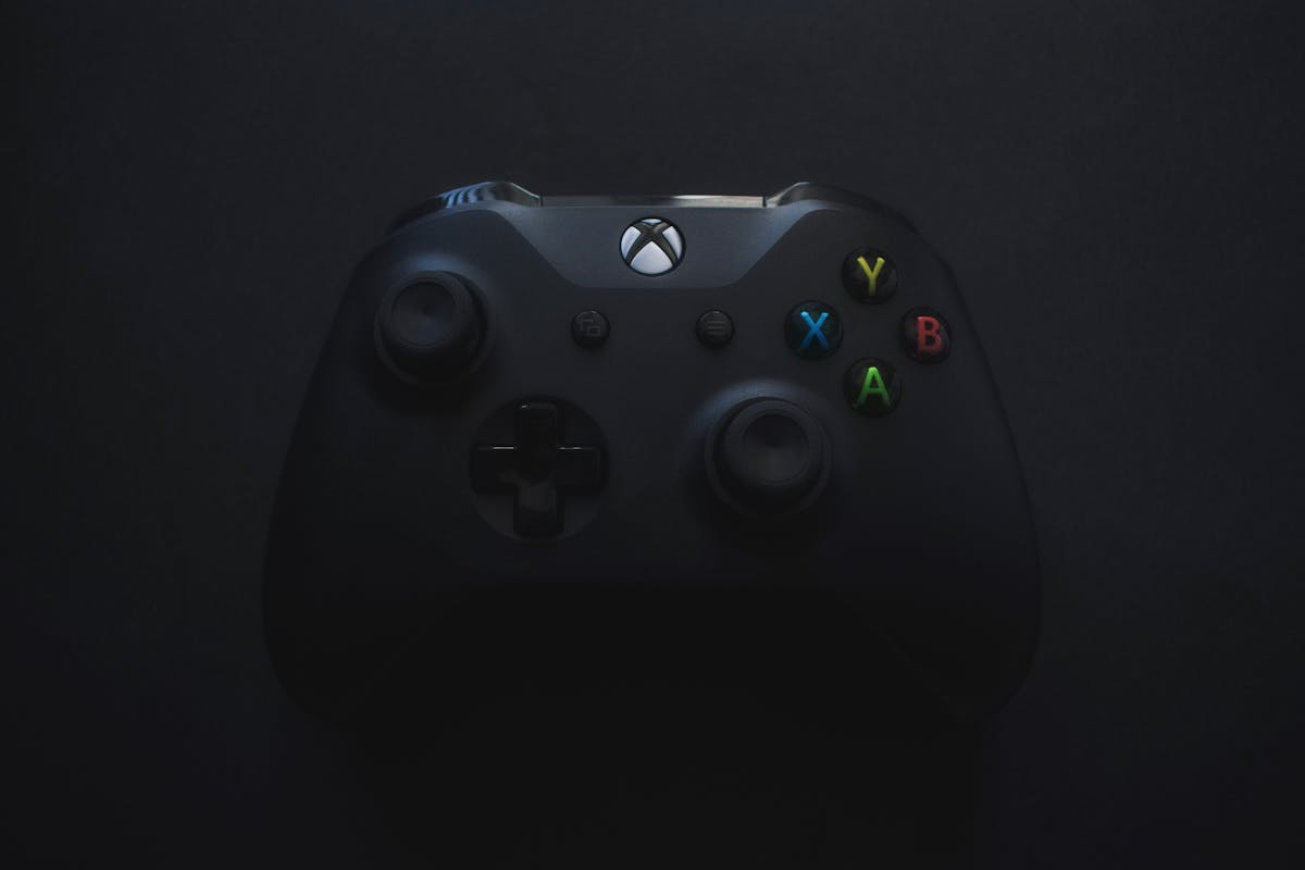
Next-Generation Portable Hardware: Architecture of Handheld Silicon and Neural Upscaling
The global anticipation surrounding the successor to the Nintendo Switch—spurred by recurring supply-chain updates and restock commentary in late October 2026—spotlights one of the most demanding sub-disciplines in computer engineering: maximizing graphics throughput and computational fidelity within a strict 10-to-15-watt handheld thermal envelope.
For nearly a decade, portable gaming hardware was constrained by legacy mobile process nodes and rasterization bottlenecks. The upcoming transition represents a generational shift, leveraging dedicated hardware tensor cores, AI reconstruction pipelines, and asymmetric docked-versus-portable clock governors.
The Handheld Thermodynamic Dilemma: 15W vs. 350W
Unlike desktop graphics cards that consume 250W to 450W with massive vapor chambers and triple-fan radiator fin stacks, a portable device must operate under strict biomechanical and thermodynamic constraints:
- Skin Temperature Threshold: The chassis where human fingers rest must not exceed 42°C (107°F) to prevent ergonomic discomfort during extended gameplay.
- Battery Capacity Limits: Lithium-ion pack regulations and aviation safety rules restrict portable batteries to under 100 watt-hours (with most handhelds targeting 40Wh to 60Wh to keep weight under 500 grams).
- Acoustic Noise Constraints: Internal centrifugal blowers cannot exceed 35 decibels without degrading audio immersion.
To achieve visual fidelity comparable to home consoles, handheld architects can no longer rely on brute-force geometry rendering. They must rely on neural temporal reconstruction.
Silicon Architecture: The Custom Heterogeneous SoC
The modern handheld compute stack integrates three interdependent silicon engines onto a single monolithic die:
flowchart TD
    subgraph Monolithic Custom SoC
        A["8x Arm Cortex-A78AE Real-Time CPU Cores"]
        B["Custom Ampere/Ada Architecture GPU (1536 CUDA Cores)"]
        C["48 Dedicated Tensor AI Cores (FP16 / INT8 / INT4)"]
        D["12GB LPDDR5X Unified Memory Controller (128-bit Bus @ 102 GB/s)"]
        E["Dedicated Display Compositor & Decompression Engine"]
    end

    A --- D
    B --- D
    C --- D
    E --- D
1. Neural Super Sampling (DLSS / Super Resolution)
Instead of rendering scenes natively at 1080p or 4K, the GPU renders geometry internally at a lower baseline resolution (e.g., 540p in portable mode or 720p in docked mode). The frame is then passed to the on-die Tensor Cores:
$$ ext{Output Pixel}(x, y, t) = mathcal{N}_{ heta}Big( ext{LowRes}(t), ext{MotionVectors}(t), ext{DepthBuffer}(t), ext{Output}(t-1)Big)$$
Where:
- $mathcal{N}_{ heta}$ is a trained deep convolutional autoencoder optimized for temporal anti-aliasing.
- The network compares multi-frame historical motion vectors to construct sub-pixel details without computational raster overhead.
// Mathematical model: Power consumption comparison between native rendering vs neural upscaling
interface RenderPowerModel {
  nativeResolutionPixels: number;
  internalRenderScale: number; // e.g. 0.5 for DLSS Performance mode
  baseGpuPowerWatts: number;
  tensorEngineOverheadWatts: number;
}

export function calculatePowerSavings(model: RenderPowerModel): {
  rasterPowerWatts: number;
  neuralUpscaledPowerWatts: number;
  powerReductionPercentage: number;
} {
  const nativePixelCount = model.nativeResolutionPixels;
  const scaledPixelCount = nativePixelCount * Math.pow(model.internalRenderScale, 2);

  const rasterPower = model.baseGpuPowerWatts;
  // Scaled rendering reduces shader ALU load quadratically
  const scaledShaderPower = model.baseGpuPowerWatts * (scaledPixelCount / nativePixelCount);
  const neuralUpscaledPower = scaledShaderPower + model.tensorEngineOverheadWatts;

  const savings = ((rasterPower - neuralUpscaledPower) / rasterPower) * 100;

  return {
    rasterPowerWatts: Number(rasterPower.toFixed(2)),
    neuralUpscaledPowerWatts: Number(neuralUpscaledPower.toFixed(2)),
    powerReductionPercentage: Math.round(savings),
  };
}
Dynamic Clock Scaling: Handheld vs. Docked Performance Profiles
To accommodate the shift between battery-constrained mobility and active wall power, the system kernel implements aggressive frequency governorship:
| Operational Mode | CPU Clock Speed | GPU Clock Speed | Memory Bus Clocks | Power Target (TDP) | Target Display Output |
|---|---|---|---|---|---|
| Handheld / Portable | 1.1 GHz (Balanced) | 450 MHz (Low-Leakage) | LPDDR5X @ 4800 MT/s | 7.5W to 9.5W | 720p / 1080p 60fps Native OLED |
| Docked in Cradle | 2.0 GHz (High Performance) | 1.0 GHz (Active Fan Boost) | LPDDR5X @ 7500 MT/s | 20W to 28W | 1440p / 4K 60fps via Tensor Upscaling |
When the device registers a cradle handshake over USB-C DisplayPort Alternate Mode, active cooling fans spin up, and the power delivery controller shifts from internal Li-ion battery draw to high-amperage USB-PD negotiation.
Long-Term Architectural Lessons for Embedded Engineers
- Memory Bandwidth is the True Wall: In heterogeneous SoCs where CPU, GPU, and NPU share a single unified pool of LPDDR5X RAM, memory contention can starve compute units. Architects must prioritize on-chip L2/L3 caches and memory compression algorithms.
- AI Cores as Efficiency Multipliers: Neural networks are no longer exclusive to cloud data centers. In edge and battery-powered hardware, specialized AI accelerators act as thermodynamic multipliers, saving battery life by replacing brute-force computation with inferred reconstruction.
Discussion (0)
Continue Reading
More production-grade engineering deep dives and architectural guides

Biggest Hack in the World: Binance Suffers Unprecedented $6.3 Billion Multi-Chain Cyberattack
A comprehensive technical autopsy of the $6.3B Binance hot-wallet breach attributed to TraderTraitor (Lazarus Group). How automated sweeping, compromised DevOps credentials, and cross-chain execution sparked the largest heist in financial history.
Mobile Push at 100M Devices: Benchmarking FCM, APNs, and Custom WebSockets
At 100M devices, push fails in the tail, not the median. We break down real delivery-latency percentiles for APNs, FCM, and owned WebSockets, plus a reproducible cost model and the reliability patterns behind 99.99%.
Landing Page Experimentation at 50M Sessions: Client-Side A/B Testing vs. Edge Decisioning vs. Server-Side Flags — Flicker, INP, and Cost per Million Decisions Benchmarked
At 50 million monthly sessions, where your A/B test makes its decision stops being a tooling preference and becomes a Core Web Vitals and P&L decision. This is a head-to-head benchmark of client-side DOM mutation, edge middleware bucketing, and server-side feature flags — measured on CLS flicker, INP, and true cost per million decisions.